Schmitt-trigger circuit tutorial
- Noise reduction with hysteresis
- Low level Schmitt trigger circuit
- Calculation of the high trigger level
- Calculation of the low trigger level
Noise reduction with hysteresis
Noise elimination is one of the main problems in achieving higher data rates and longer communication cables. There are several ways noise can be reduced. Communication lines can be shielded. Differential communication like with RS422 and RS485 is quite immune to noise, especially when the wires are twisted. Low output impedance and proper termination resistors to reduce reflections may also help, but there will always be some noise left on the line. This noise can be reduced by adding input filters, for example with an RC network, but input filters have the disadvantage that they not only reduce noise, but also the maximum allowed data rate. Another possibility is adding a hysteresis in the input line. An input line with hysteresis uses two switching levels Vhigh and Vlow. When the input voltage exceeds Vhigh, the output switches to a high level. Only when the input voltage falls below Vlow (which should be lower than Vhigh), the output switches back to its low state. This type of noise reduction is implemented in the inputs of the I²C bus. The effect of an hysteresis can be seen in the next picture.
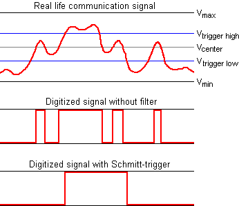
The first graph shows the actual input signal. There is quite some noise on the line, and if the center voltage is used to determine if the input is in the on, or off state, there can be four high periods detected in the signal as shown in the second graph. If we however use two trigger levels with hysteresis, it is possible to reduce the number of detected logical highs to only one. This is what the Schmitt trigger does in the last graph.
Low level Schmitt trigger circuit
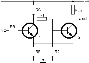
Making an electronic circuit with hysteresis is not difficult, thanks to Otto Schmitt, an American scientist. He invented a simple electronic circuig which has a built-in hysteresis effect. This circuit is now known as the Schmitt-trigger. Two transistors and a handful of carefully chosen resistors are enough to create the circuit. The values of the resistors define the input voltage levels where the Schmitt trigger circuit changes state. The basic Schmitt trigger circuit is shown in the next picture.
Calculation of the high trigger level
Let’s try to understand this circuit by assuming the input voltage is zero. Transistor T1 will not conduct because of the zero input voltage. The state of transistor T2 is totally determined by the resistors RC1, R1 and R2. These three resistors create a voltage divider. Let’s assume that the base current flowing in T2 is small enough to be neglected. With modern transistors where the gain hFE is often larger than 150 this assumption will create only a very small error. The base voltage of T2 can then be calculated as
VB2 = Vsupply * R2/(RC1+R1+R2)
The emitter voltage of T2 will be less, because of the VBE voltage difference between the base and emitter. For a silicon transistor where current is flowing, the VBE voltage can be estimated at roughly 0.61 Volt. The emitter voltage can be calculated as:
VE2 = VB2 – VBE2 = Vsupply * R2/(RC1+R1+R2) – 0.61
The Schmitt trigger circuit uses emitter coupled logic. Therefore VE = VE1 = VE2.
Now consider the situation that the input voltage of the circuit increases. As soon as VB1 is larger than VE1, a very small current will start to flow through transistor T1. This current also passes resistor RC1, and therefore the base voltage of transistor T2 will decrease. As the base voltage gets lower, so does the emitter voltage of transistor T2 and because the emitters of transistor T1 and T2 are directly coupled, the voltage difference VBE1 will increase. More current will start to flow through transistor T1 and transistor T2 will close. Please note that the emitter voltage over resistor RE won’t fall to zero. Although T2 is closing, T1 is opening at the same time keeping the emitter voltage more or less stable at a value of Vin – VBE. When T2 is totally closed and T1 has opened, the system has changed state. The output will change to the high state because resistor RC2 pulls the output to the power supply. The trigger voltage where this effect starts to happen is called the high trigger voltage and can be approximately calculated as
Vhigh = Vsupply * R2/(RC1+R1+R2) – 0.61
It is evident that an increasing voltage at the input of the circuit will keep the circuit in the high state. This is because a higher voltage at the input will create a higher base and collector current and this higher collector current will pull the base voltage of transistor T2 even further down. But when does the circuit fall back to its zero state again? This requires further analysis of the circuit.
Calculation of the low trigger level
If Vin is lowered, the current flowing through T1 will decrease. This causes the current through resistor RC1 to decrease and the voltage level at the base of transistor T2 will increase. Because the transistors are emitter coupled, the emitter voltage of that transistor decrease, and when Vin is low enough, the base voltage of transistor T2 will become slightly higher than the emitter voltage, causing a small base current to flow through T2. This small base current will create an emitter current through the shared resistor RE. The emitter voltage will rise and less current will flow through T1 because the voltage difference between the base and emitter of T1 gets smaller. This causes less current to flow through RC1 and the base voltage at T2 increases even more. T2 will open and T1 will close at the same time. At this input level Vin the circuit has changed state back to zero. But at what specific voltage is this state change triggered?
Calculating the low trigger voltage for a Schmitt trigger circuit is a little bit more difficult than calculating the high trigger level. T2 will start to open when the base voltage VB2 gets slightly larger than the emitter voltage VE2. We will try to calculate the input voltage where VB2 and VE2 are equal when T2 is
closed.
First some basic calculations for voltages and currents in the circuit when T2 is closed. As stated above, we assume that the base currents flowing through the transistors are small. Therefore the collector current and emitter current through T1 are considered equal. Also because T2 is closed, there won’t flow any base current through this transistor.
VE = IE1 * RE
VC1 = IR1R2 * (R1+R2)
Vsupply – VC1 = (IC1 + IR1R2) * RC1
The important factor in this calculation is the collector voltage of transistor T1, because if we know this value we can easily calculate the base voltage of transistor T2. Given the above equations and the assumption that IE1 equals IC1, we can derive
VC1 = Vsupply – RC1 * (VE/RE + VC1/(R1+R2))
VC1 is still on both sides of the equation, but this can be solved with some simple mathematics. This gives:
VC1 = (Vsupply – VE * RC1/RE) / (1 + RC1/(R1+R2))
With this equation, we can easily calculate the voltage level VB2 of the second transistor.
VB2 = VC1 * R2/(R1+R2)
VB2 = (Vsupply * R2 – VE * RC1*R2/RE) / (RC1+R1+R2)
This is where the magic jumps in. We are looking for the value of VB2 where the transistor T2 starts conducting. This is the point where the base voltage VB2 equals the emitter voltage VE. We can therefore substitute VE for VB2 and reduce the equation further. I will skip some steps, but the end-result can be shown below:
VE = Vsupply * R2/(RC1+R1+R2 + RC1*R2/RE)
When transistor T2 starts to conduct, the transistor T1 is still open, so the calculate the input voltage where T2 starts to conduct, we have to add VBE or 0.61 Volt to this equation to calculate the value at the base port of T1. The low trigger value of the Schmitt trigger can therefore be calculated as
Vlow = Vsupply * R2/(RC1+R1+R2 + RC1*R2/RE) + 0.61
|
To err is human;
to blame it on someone else
is even more human.
JACOB'S LAW
|